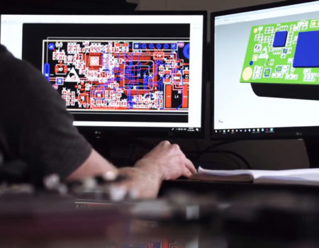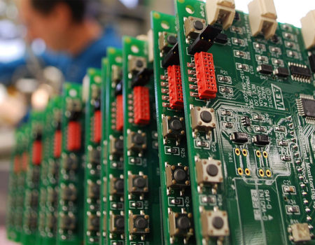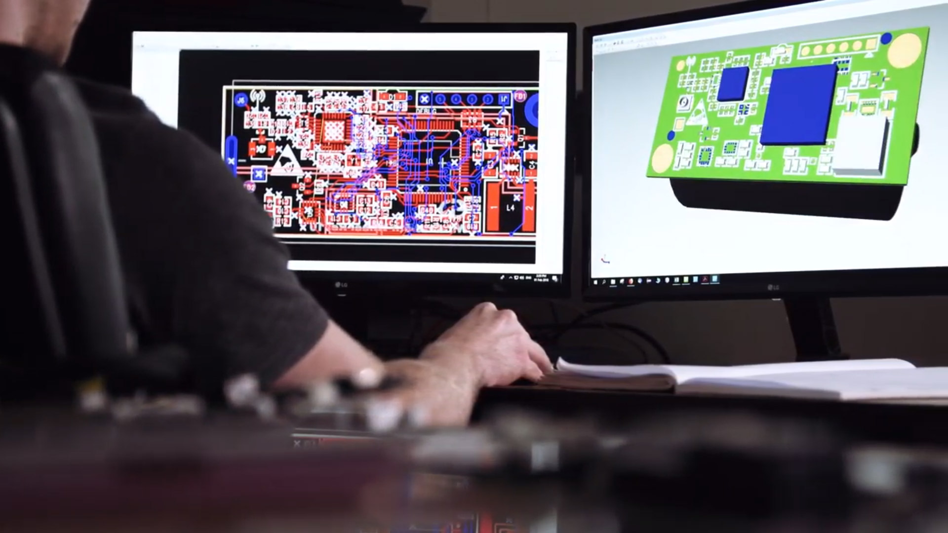
When CAO routing an electronic board with fast signals, it is important to proceed in stages and analyze them. Indeed, it is necessary to understand the operation of the electronic card in order to be able to implant it correctly. Each component of the electronic board must have a specific location. It is necessary to calculate with precision the impedances of the differential transmission lines for the operation of these. HDI routing is imperative, and therefore represents a critical point during the design of the electronic card and thus adds an additional constraint. To provide more precision during the CAD routing phase with fast signals, for example, Expert PCB uses the Altium designer software. It allows, for example, to integrate the 3D image into a printed circuit to optimize its integration.
Here are the main steps in the design of an electronic card with fast circuits:
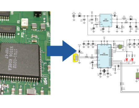
Step 1 – Analyze the component datasheet.
Step 2 – Depending on the component, we can find several cases
- Differential pairs with a given impedance
- Simple links with a given impedance
- A single link bus with a given impedance but the same length as those cis.
Step 3 – Analyze the impedances in the component datasheet.
the most common impedances are 50 ohms, 80 ohms, or 100 ohms.
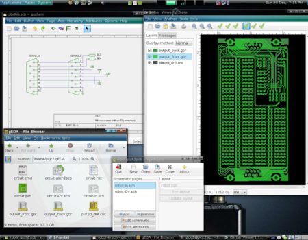
Step 4 – After analyzing the components and the complexity of the diagram we define the printed circuit with the number of layers necessary for the routing of these signals and on which layers these signals go.)
Step 5 – Depending on the stacking chosen and the impedances there are calculations to be carried out to define the widths of the links layer by layer. There are several cases
Expert PCB puts at your disposal his knowledge and his know-how for the routing of your electronic boards. Expert in this sector for more than 15 years we support you in all stages of your project.
Our other posts