Expert pcb - Electronic CAO study office

  • PCB CAD process
  • design steps
  • ISO9000 Quality

MAITRISE DES PROCESSUS DE CONCEPTION

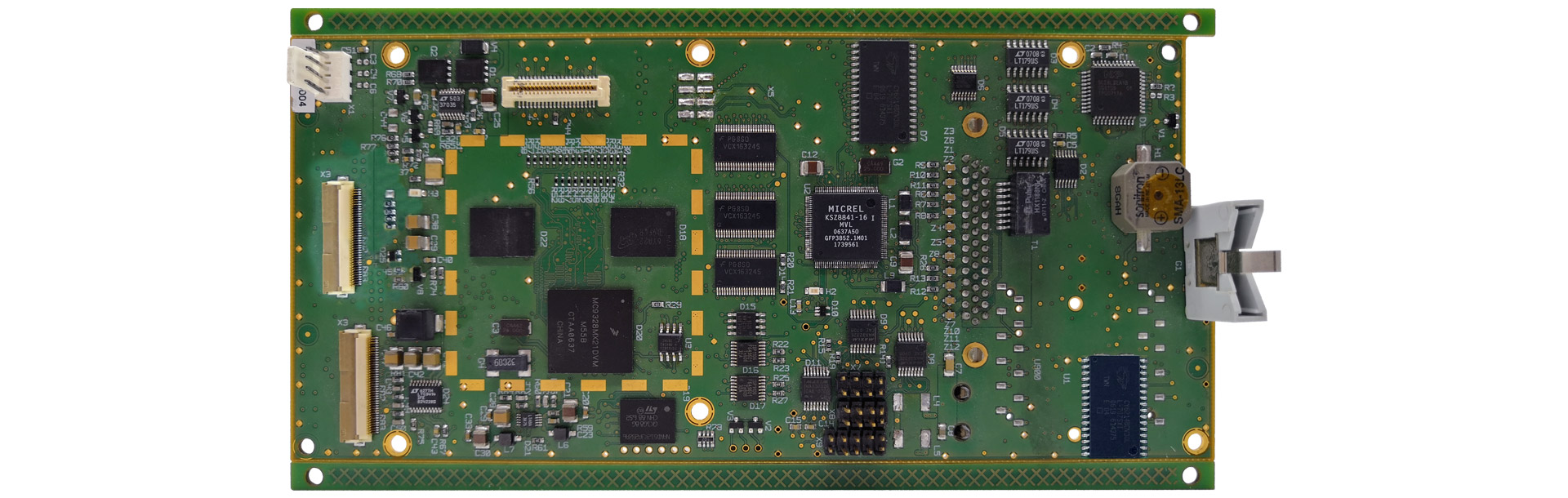
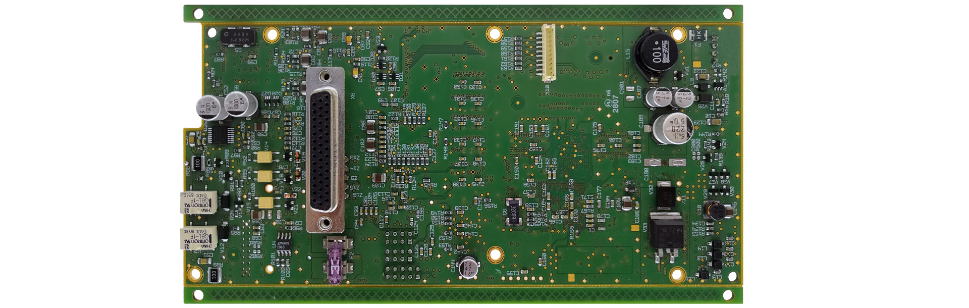
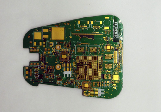
During electronic CAO subcontracting, we follow a rigorous process for the study and electronic routing of your card. At each key stage, our team of implanters validates the work with you: diagrams, placement, routing, DRC, adapted impedance and HDI, manufacturing and assembly file.

Phases of electronic CAO subcontracting

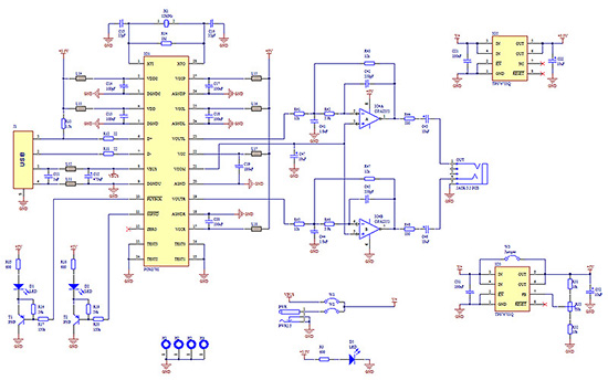
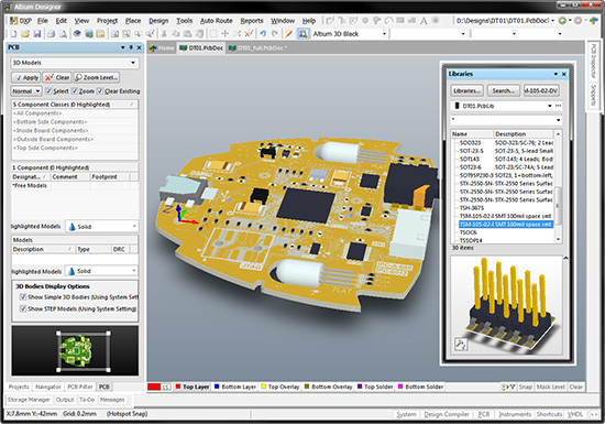
Based on your data and technical specifications, we will set up a rigorous and quality PCB CAD design process. Our electronic CAO stations allow us to import netlists from other CAD software such as: Altium Designer, Cadstar, Eagle, Cadence, Visula, Orcad, etc.

PCB design process

Kick Off

Formalization of the order by submitting your final specifications: diagrams, layers, BOM, routing rules, mechanical plans, design standard, etc. A checking of the input data is carried out. Updating of schemas is permitted. The technical inconsistencies are resolved.

Update Schéma

Analysis: inconsistencies, labels, power supplies, disconnection, etc …

PCB library creation

Pads specific to components not listed in the CAD editor database must, in some cases, be designed by our technicians. Editing your PCB in 3D format can also be one of your concerns.

Placement

Validation of the diagram and placement of components. This is a crucial step for routing. Care is taken to place the decoupling capacitors as close as possible to the power supplies.

Routing

Routing, rule initialization, stackup, CEM table, etc.
Isolation routing. Routing of critical tracks.
Ground plane routing.
Finishing and silkscreen printing.

MFG files

Creation of CAM files Gerbers, drill, mill, P & amp; P, etc …
Documentation.
Database, DFX, pdfs.
Standard file with plans and CD.

Electronic diagram - Expert PCB
Expert PCB Altium
PCB - Altium Layout - EXPERT PCB
NEED A CAD PCB STUDY?

Exemple de carte CPU MC24 FR4 16/10 HDI impédance contrôlée

  1. Certifications cartes électronique - Recto
  2. Certifications cartes électronique - Verso
  • Electrolytic gold plating:Ep Nickel 5 μm, Ep, Or 0,1 à 5 μm
  • Chemical gilding: Ep Nickel 3 à 5 μm, Ep, Or 0,05 à 0,10 μm
  • Copper deposit: 30 à 35 μm maxi
  • Gold plating Connector and Rubbing contacts: Ep Nickel 3 à 7 μm , Or Cobalt 2 μm mini
  • Gilding on bare copper: 3 μm Mini

Testimonials

EXPERT PCB :
Sous-traitance CAO électronique

+33 (0)4.28.61.78.43

99 CHEMIN DES HUGUENOTS - 26000 VALENCE

contact@expert-pcb.com