Since its creation in 2007, Expert PCB has carried out for 500 customers more than 1500 electronic Layout Design as well as PCB designs on all routing stations.
For our French and European customers, we carry out the PCB layout of electronic boards. In fact, from entering the diagrams to importing netlists, we route the maps. By using all the technologies certified with our PCB manufacturing partners but also EMS for assembly. Also our knowledge and experience of electronic CAD study allow you to be confident for your electronic board project.
This internal know-how gives us a strong reactivity when modifying the electronic card. For example for new dimensions, a new environmental constraint or a change of component; Our internal teams can directly readjust the routing of the boards.
Customers
Finalized projects
PCB manufactured
ELECTRONIC CAD SOFTWARE USED
Our PCB CAD stations allow us to import netlists from other CAD software such as: Altium Designer, Cadstar, Eagle, Cadence, Visula, Orcad, CR5000, Kikad, Proteus…


High Tech PCB Technologies
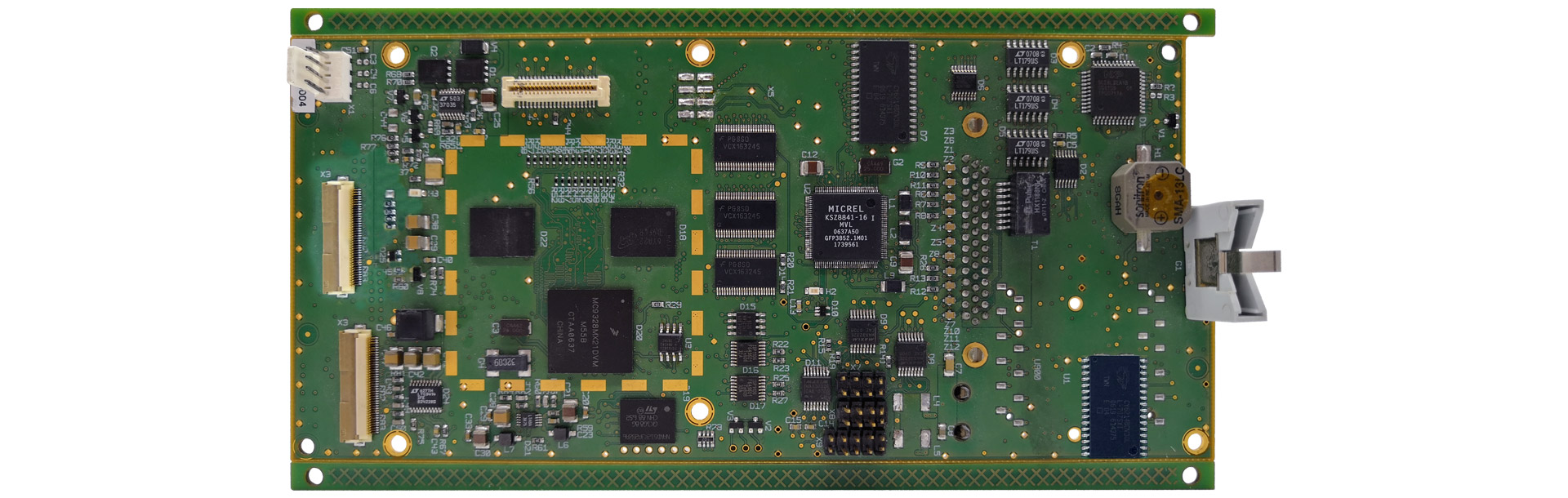
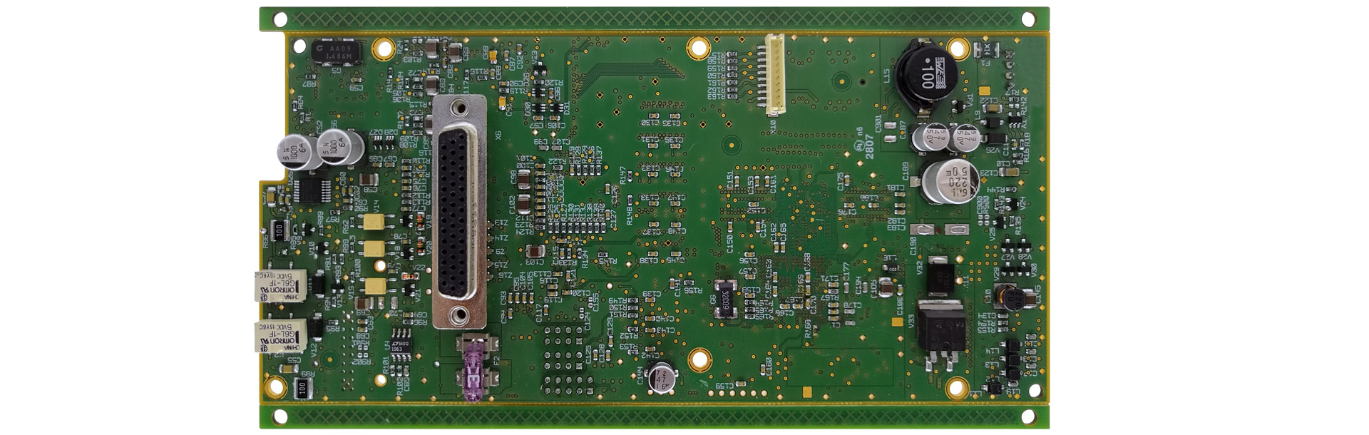
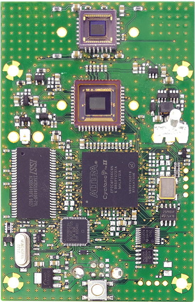
The trend towards the miniaturization of electronics has not stopped. Indeed, the use of BGA, µBGA which are components more and more small and having electronic operating speeds more and more fast requires an obvious routing expertise. Whether it is Rigid, Flex, Flex-Rigid or FR4 Semiflex PCB. Expert PCB therefore uses the technologies that suit your electronic board project. Our experienced implanters support you from the development phase.
Need an electronic design quote?
ISO / IPC Standards and Certifications
When an electronic board has been properly produced in CAD, 80% of the development problems will be solved, all technicians and engineers know this well. Indeed, our completed projects have enabled us to capitalize on numerous routing and manufacturing standards and rules. Because we update them every day with our global PCB partners but also with EMS so that the whole production process is as perfect as possible.